Breaking Barriers in AI Computation: The Rise of Photonic Processors
As the demands of modern machine-learning applications surge, traditional electronic computing hardware is being stretched to its limits. Enter photonic hardware—a groundbreaking alternative that harnesses light to perform machine-learning computations at blazing speeds while consuming significantly less energy.
However, until now, photonic devices faced limitations in executing certain neural network computations, necessitating off-chip electronics that reduced their efficiency. This critical challenge has been addressed by a cutting-edge photonic chip, developed by researchers at MIT and beyond, which promises to revolutionize the landscape of artificial intelligence.
A Fully-Integrated Photonic Processor
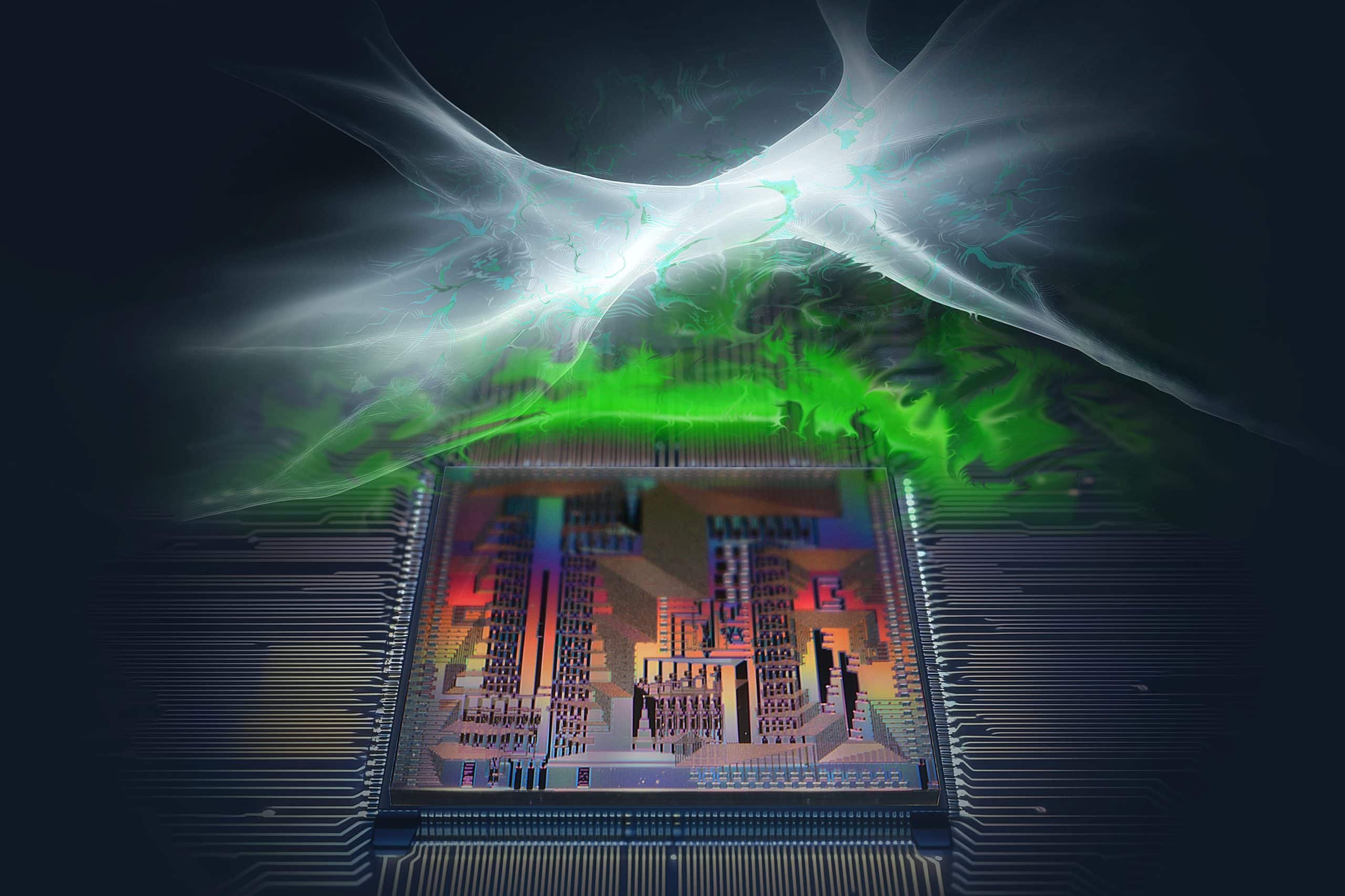
Building on over a decade of research, scientists have unveiled a photonic processor capable of performing all vital computations of a deep neural network entirely on-chip. This groundbreaking device demonstrated its prowess by completing key machine-learning classification tasks in under half a nanosecond, achieving over 92% accuracy—on par with traditional hardware solutions.
The chip leverages interconnected modules to create an optical neural network. Manufactured using commercial foundry processes, this innovation paves the way for scalable production and seamless integration into existing electronics.
From Linear to Nonlinear: Overcoming Photonic Challenges
Deep neural networks rely on layers of interconnected nodes to process data. While linear operations like matrix multiplication are straightforward for photonic systems, nonlinear functions, essential for identifying intricate patterns, posed a significant challenge.
In 2017, researchers demonstrated an optical neural network capable of matrix multiplication using light. However, the inability to perform nonlinear operations on-chip meant relying on digital processors—a bottleneck in efficiency. To overcome this, the team introduced Nonlinear Optical Function Units (NOFUs), which combine optics and electronics to handle nonlinear tasks directly on the chip, ensuring ultra-low power consumption and seamless operation.
Unprecedented Performance and Energy Efficiency
The photonic processor achieved over 96% accuracy during training and more than 92% during inference. Its ability to perform computations in less than half a nanosecond opens new avenues for applications requiring real-time decision-making, such as navigation, telecommunications, and scientific research.
Additionally, the efficiency of in situ training on the chip—a process that traditionally consumes vast amounts of energy in digital systems—marks a significant leap toward sustainable AI. For further reading on the environmental impact of AI and innovative solutions, check out The Environmental Impact of AI: Solutions for a Sustainable Future.
Scaling AI with Photonics
The researchers employed CMOS-compatible manufacturing processes to fabricate the chip, ensuring minimal errors and compatibility with existing electronic systems. Looking ahead, the focus will shift to scaling this technology and integrating it with real-world applications like cameras, LIDAR systems, and high-speed communication networks.
Moreover, the team aims to refine algorithms that exploit the unique advantages of optics for faster, more energy-efficient training of AI systems. This innovation could redefine industries ranging from particle physics to next-generation telecommunications.
A Vision for the Future
With funding from the U.S. National Science Foundation, the U.S. Air Force Office of Scientific Research, and NTT Research, this breakthrough sets the stage for a future where photonics drives the next wave of artificial intelligence. The photonic processor represents a monumental shift, enabling AI computations at speeds and efficiencies previously thought unattainable.